 "Representational image. Reuters")
The Electronics Component Manufacturing Scheme has received investment proposals worth Rs 1.15 lakh crore, Union Minister for Electronics and IT Ashwini Vaishnaw said on Thursday.
He said the proposals have exceeded investment, employment and production targets multifold when compared to the goals set during formulation of the scheme.
“Application window for Electronics Component Manufacturing Scheme closed on September 30. We have received investment proposals of Rs 1,15,351 crore,” Vaishnaw said.
He said that the government has envisaged getting investment of around Rs 59,000 crore under the scheme and that the application window for capital equipment segments is still open.
Electronics and IT Secretary S Krishnan said the proposals promise to generate employment for 1.41 lakh persons compared to target of 91,600 persons envisaged under the scheme.
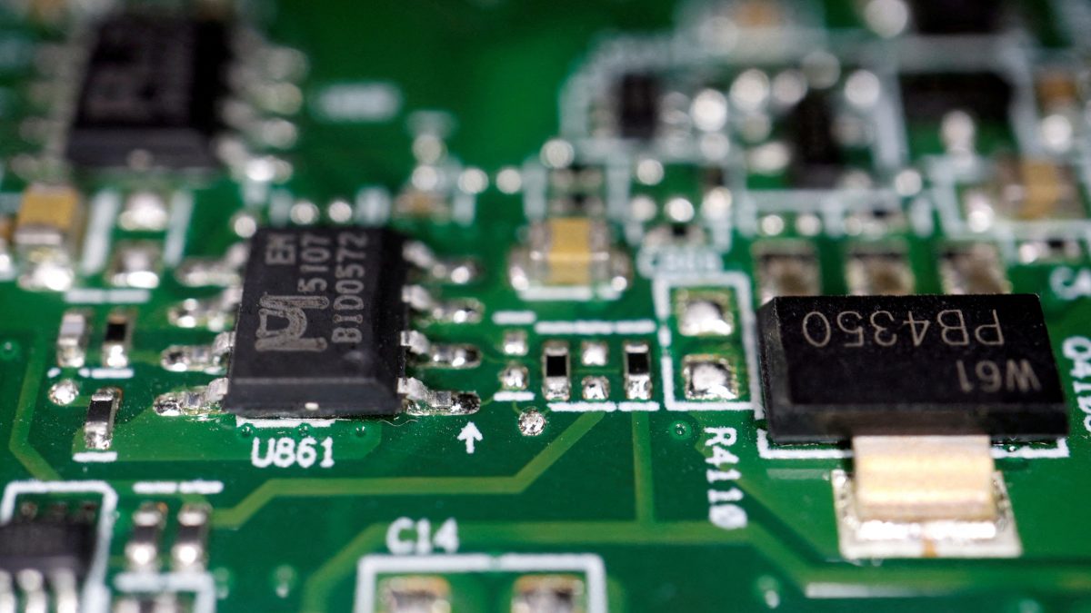
On April 8, 2025, the Government of India officially notified the Electronics Component Manufacturing Scheme (ECMS), a forward-looking initiative designed to deepen the nation’s capabilities in electronics manufacturing.
While previous schemes such as Semicon 1.0, Semicon 2.0, the Production Linked Incentive (PLI) for Large-Scale Electronics Manufacturing (LSEM) and the PLI for IT Hardware had already accelerated India’s entry into global electronics supply chains, they were largely focussed on assembly, design and large-scale production.
The ECMS represents a crucial next step in building a strong and resilient ecosystem for the manufacturing of components themselves.
This move is timely as India is emerging as one of the fastest-growing electronics manufacturing destinations in the past decade with mobile production rising at a compound annual growth rate of 24 per cent and exports increasing at an even more remarkable 57 per cent.
Impact Shorts
More ShortsHowever, the full strength of the industry can only be realised if domestic capacity in key components is established. The ECMS directly addresses this gap by encouraging large-scale investments, innovation and global linkages in component manufacturing.
Scheme structure and tenure
The scheme has been structured with a tenure of six years and allows for a one-year optional gestation period to help companies stabilise their operations before scaling production.
It carries a significant budget outlay of Rs 22,919 crore ($2.7 billion).
This financial commitment reflects the government’s ambition to not only attract manufacturing investments but also to enhance domestic value addition (DVA) and integrate India’s electronics sector more deeply into Global Value Chains (GVCs).
Objectives
The ECMS was designed with two overarching objectives. The first is to develop a robust and competitive ecosystem for the manufacturing of electronics components within the country. This would reduce import dependence and strengthen the foundations of the industry.
The second objective is to expand India’s share in global electronics trade by integrating the domestic sector into international supply chains, thus positioning the nation as a trusted partner for advanced component manufacturing across the world.
Targets and early outcomes
At its inception, the scheme set ambitious goals.
The targets included attracting investments worth Rs 59,350 crore (approximately $7 billion), achieving production of Rs 4,56,500 crore ($53.7 billion), and generating employment for 91,600 people. However, within months of its launch, the industry response far exceeded expectations.
The following table presents a comparison between the original targets and the outcomes expected on the basis of applications received by September 30, 2025:
This remarkable over-subscription highlights the depth of confidence the industry places in India’s policy stability, its growing domestic market and its emerging role as a global manufacturing hub.
Application windows
The scheme invited applications in multiple segments of component manufacturing. The windows for target segments A, B, C and E closed on September 30, 2025, while the window for segment D will remain open until April 30, 2027, providing a two-year period for further applications.
The ministry has already initiated the scrutiny of eligible applicants and has assured that the approval process will be fast-tracked in order to sustain industry enthusiasm.
Segment-wise applications and investments
The industry response has been diverse, with applications received across critical categories of electronics manufacturing.
By the end of September 2025, a total of 249 applications had been filed with a proposed investment of Rs 1,15,351 crore. These investments span a range of component categories, including both traditional areas and new technology-driven segments.
For instance, display module sub-assembly attracted twenty-two applications with proposed investments of Rs 8,642 crore, while camera module sub-assembly received fourteen applications worth Rs 6,205 crore.
Non-SMD passive components drew 15 applications with Rs 1,608 crore of proposed investment and electro-mechanicals witnessed the highest participation with eighty-seven applications totalling Rs 14,362 crore. Multi-layer printed circuit boards (PCBs), another essential segment, attracted 43 applications worth Rs 14,150 crore.
In high-value areas, the response was equally strong.
Li-ion cells for digital applications, excluding storage and mobility, brought in four applications worth Rs 4,516 crore. Enclosures for mobile devices, IT hardware products and related devices attracted 16 applications, but with the largest proposed investment of Rs 35,813 crore, making this the single largest sub-sector in terms of financial commitment.
High-density interconnect (HDI), modified semi-additive process (MSAP) and flexible PCBs saw 11 applications totalling Rs 16,542 crore.
Smaller but significant responses came for SMD passive components, with two applications worth Rs 535 crore, and optical transceivers (SFP), with nine applications totalling Rs 1,645 crore. Additionally, eighteen applications worth Rs 9,226 crore were submitted for the supply chain of sub-assemblies and bare components, and eight applications worth Rs 2,103 crore were received for capital goods used in electronics manufacturing.
Key highlights and strategic significance
The ECMS is notable not only for the scale of participation but also for several first-time developments. For the first time, significant investments have been committed in areas such as SMD passive components, laminates, flexible PCBs, anodes and capital equipment.
This diversification is critical for reducing India’s dependency on imports and for establishing a complete value chain domestically.
Another highlight is the highest-ever single-company investment commitment of approximately Rs 22,000 crore, signalling a major vote of confidence by global industry leaders.
The unprecedented scale of applications and the quantum of proposed investments reflect growing confidence in India’s stable and transparent policy environment.
The scheme is also the result of extensive stakeholder consultations, ensuring that industry concerns were addressed and that the scheme’s design aligns with both government priorities and industry realities.
The ECMS is therefore more than just an incentive programme and represents a collaborative effort to make India self-reliant in electronics manufacturing while simultaneously boosting its global competitiveness.
Contribution to the national vision
The ECMS is central to the prime minister’s vision of establishing a $500 billion domestic electronics manufacturing ecosystem by 2030-31.
By creating a strong base for component manufacturing, the scheme strengthens India’s ability to withstand global supply chain disruptions, promotes domestic research and development in critical technologies and enhances its ability to compete in the export market.
It is also a powerful engine for job creation, offering more than 1.4 lakh employment opportunities as per current estimates and thereby supporting inclusive economic growth.