
 "India boosts semiconductor manufacturing with Rs 4,600 cr Cabinet approval for 4 new units")
The Union Cabinet, led by Prime Minister Narendra Modi, authorised four additional semiconductor manufacturing projects on Tuesday, totalling Rs 4,600 crore under the India Semiconductor Mission (ISM).
The initiatives will increase local manufacturing of chips, packaging, and innovative materials, creating approximately 2,000 skilled jobs immediately.
Two of the four approved projects are located in Odisha, one in Punjab, and one in Andhra Pradesh.
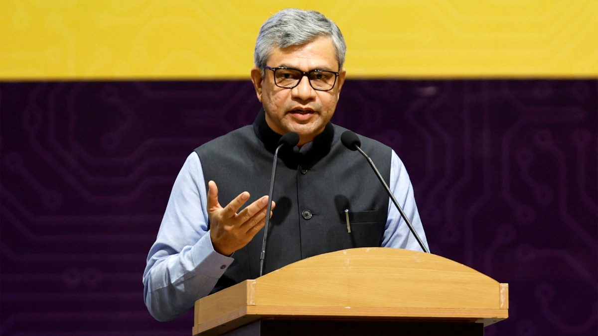
“Four new semiconductor projects have been approved. You know that six projects are already approved and four new ones have been added to it today. These are in Odisha, Andhra Pradesh and Punjab, at an investment of Rs 4,594 Crore,” Union Minister Ashwini Vaishnaw said at a press conference in New Delhi today.
The approvals bring the whole India Semiconductor Mission (ISM) portfolio to ten projects across six states, with a combined investment of Rs 1.6 lakh crore. The government stated that the action is consistent with its objective of developing a robust and self-sufficient semiconductor ecosystem to assist industries ranging from military to consumer devices.
Two of the approved projects will be developed in Odisha’s Info Valley, Bhubaneswar, establishing the state as an emerging hub for the industry.
SiCSem Private Limited will establish the country’s first commercial compound semiconductor manufacturing factory, capable of generating 60,000 wafers per year and packaging 96 million units. The plant’s goods will find use in electric cars, railroads, rapid chargers, data centres, solar inverters, consumer appliances, and missile systems.
The second Odisha project, by 3D Glass Solutions Inc. (3DGS), will establish an advanced packaging and embedded glass substrate facility. It will introduce the world’s most advanced semiconductor packaging technology to India, with an annual capacity of 69,600 glass panel substrates, 50 million assembled units and 13,200 3D Heterogeneous Integration (3DHI) modules. The technology will be used in high-performance computing, artificial intelligence, defence electronics, radio frequency and photonics applications.
Impact Shorts
More ShortsIn Andhra Pradesh, Advanced System in Package (ASIP) Technologies, in collaboration with South Korea’s APACT Co. Ltd., will set up a semiconductor manufacturing unit with a capacity of 96 million units a year. The plant will serve markets for mobile devices, set-top boxes, automotive electronics and other applications.
The fourth project that was approved by the Union Cabinet is for Continental Device India Ltd. (CDIL) in Mohali, Punjab, it will expand the company’s discrete semiconductor manufacturing capacity. The upgraded facility will produce 158.38 million units of high-power devices annually, including MOSFETs, IGBTs, Schottky diodes and transistors in both silicon and silicon carbide. These components are used in EV electronics, renewable energy systems, power conversion, industrial automation and communication infrastructure.
The approvals mark a decisive step in positioning India as a global semiconductor hub. “These projects will accelerate our journey towards Atmanirbhar Bharat in electronics manufacturing and create a talent pool that will serve global industry,” the government said in a statement.
The ISM has already attracted major investments and fostered a growing design ecosystem, with 72 startups and 278 academic institutions engaged in semiconductor R&D and training. Over 60,000 students are benefitting from semiconductor talent development programmes across the country.

 "Russian drones over Poland: Trump’s tepid reaction a wake-up call for Nato?")
 "As Russia pushes east, Ukraine faces mounting pressure to defend its heartland")
 "Why Mossad was not on board with Israel’s strike on Hamas in Qatar")
 "Turkey: Erdogan's police arrest opposition mayor Hasan Mutlu, dozens officials in corruption probe")


