
 "TSMC exploring options to set up highly sophisticated chip fabrication plant in Japan")
Taiwan Semiconductor Manufacturing Co, TSMC is reportedly planning to set up an advanced silicon packaging capacity in Japan, sources familiar with the matter disclosed, signalling a potential stride in Japan’s semiconductor industry revitalization efforts.
The discussions are in preliminary stages, the sources noted, opting to remain anonymous due to the non-public nature of the information. One avenue being explored by the semiconductor behemoth involves the introduction of its chip-on-wafer-on substrate (CoWoS) packaging technology to Japan, as revealed by one source briefed on the matter.
CoWoS, a cutting-edge technology, entails stacking chips atop one another, thereby enhancing processing capabilities while conserving space and reducing power consumption. Presently, all of TSMC’s CoWoS capacity resides in Taiwan. No definitive decisions regarding the scale or timeline of potential investments have been reached, according to the source. TSMC, formerly known as Taiwan Semiconductor Manufacturing Co., declined to provide comments on the matter.
Global demand for advanced semiconductor packaging has surged in tandem with the artificial intelligence boom, prompting chipmakers like TSMC, Samsung Electronics, and Intel to ramp up capacity.
TSMC’s Chief Executive C.C. Wei announced plans in January to double CoWoS output this year, with further expansions slated for 2025. Meanwhile, TSMC divulged intentions to augment advanced packaging capacity in Chiayi, southern Taiwan, to meet robust market demand, albeit without specifying details.
Construction of a new CoWoS facility in Chiayi is scheduled to commence in early May, as per statements attributed to Vice Premier Cheng Wen-tsan by Taiwan’s Central News Agency.
Impact Shorts
More ShortsBy bolstering advanced packaging capabilities, TSMC aims to extend its footprint in Japan, where it recently inaugurated one plant and announced another, both situated on the southern island of Kyushu, a pivotal chipmaking hub. TSMC has forged partnerships with firms such as Sony and Toyota, with total investments in the Japanese venture anticipated to exceed $20 billion.
Moreover, TSMC established an advanced packaging research and development center in Ibaraki prefecture, northeast of Tokyo, in 2021. Japan’s robust semiconductor materials and equipment ecosystem, coupled with burgeoning investments in chip fabrication capacity and a stable customer base, positions the country favorably to assume a larger role in advanced packaging, noted a senior official at Japan’s industry ministry.
However, TrendForce analyst Joanne Chiao cautioned that TSMC’s potential advanced packaging venture in Japan might be constrained in scale, as demand for CoWoS packaging within Japan remains uncertain. Most of TSMC’s current CoWoS customers are based in the United States, Chiao added.
TSMC’s endeavours in Japan thus far have been buoyed by substantial subsidies from the Japanese government, which views semiconductor production as integral to its economic security following setbacks vis-à-vis South Korea and Taiwan.
Concurrently, Intel is reportedly contemplating the establishment of an advanced packaging research facility in Japan to deepen collaborations with local chip supply chain firms, according to sources familiar with the matter. Samsung, meanwhile, is setting up an advanced packaging research facility in Yokohama, southwest of Tokyo, with government backing. Additionally, the South Korean chipmaker is engaging in discussions with Japanese and other companies regarding material procurement as it endeavours to leverage packaging technology to catch up in high-bandwidth memory chips, as reported by Reuters.
(With inputs from agencies)

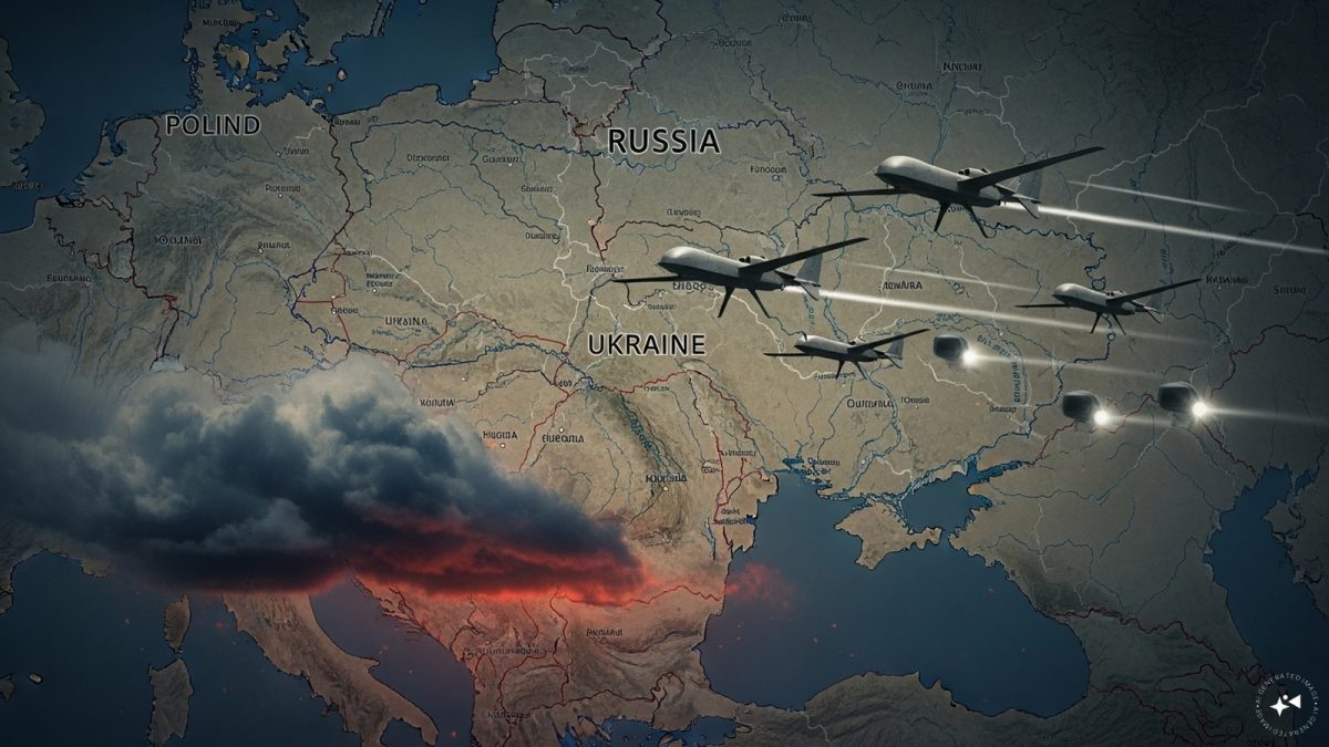 "Russian drones over Poland: Trump’s tepid reaction a wake-up call for Nato?")
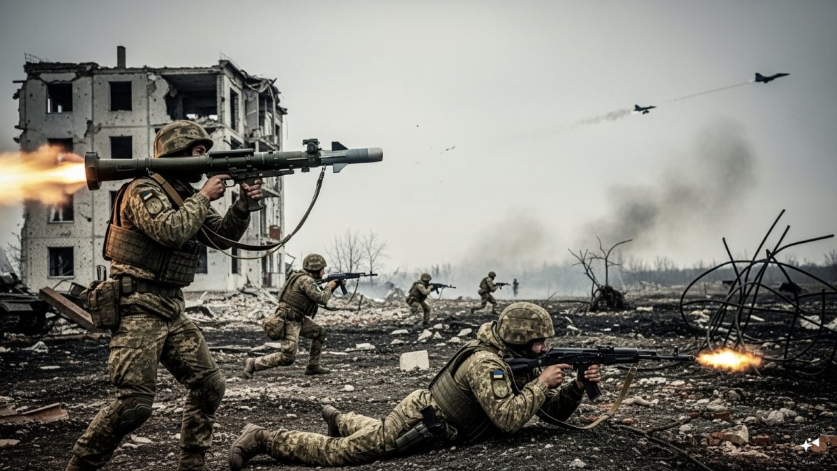
 "As Russia pushes east, Ukraine faces mounting pressure to defend its heartland")
 "Why Mossad was not on board with Israel’s strike on Hamas in Qatar")
 "Turkey: Erdogan's police arrest opposition mayor Hasan Mutlu, dozens officials in corruption probe")
 "Russian drones over Poland: Trump’s tepid reaction a wake-up call for Nato?")
 "As Russia pushes east, Ukraine faces mounting pressure to defend its heartland")
 "Why Mossad was not on board with Israel’s strike on Hamas in Qatar")
 "Turkey: Erdogan's police arrest opposition mayor Hasan Mutlu, dozens officials in corruption probe")


